Connectors & IO PINS
GPIO (SensForge Board)
The GPIO Expansion Header on the SensForge board provides direct access to Pulsar General Purpose I/O pins, allowing you to connect custom sensors, actuators, and other external peripherals for rapid prototyping. The header exposes a combination of digital I/O pins, analog inputs from the front-end ADC, and system control signals.
Pinout Diagram
The 24-pin expansion header is arranged as shown in the diagram below.
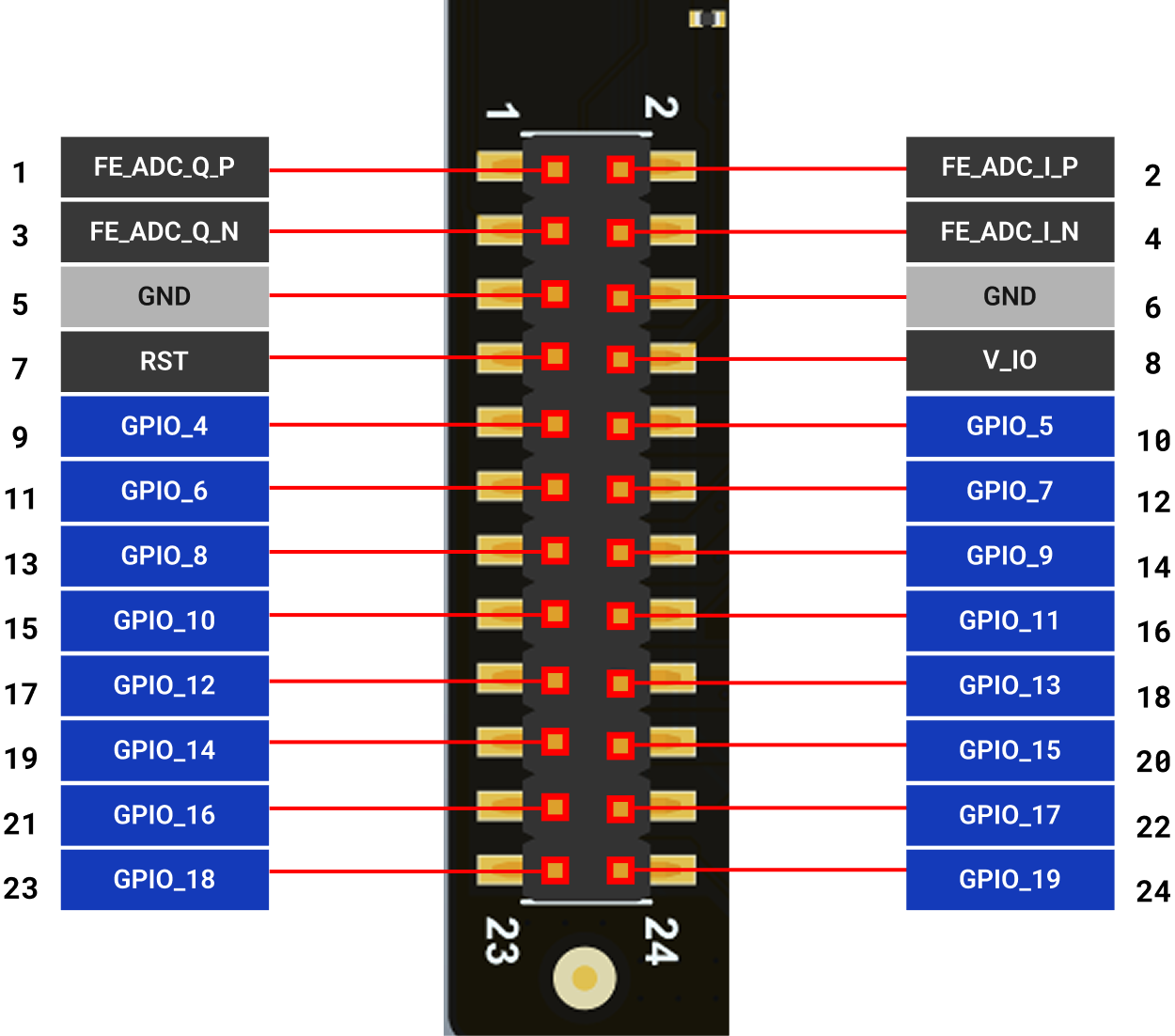
Pin Descriptions
The following table provides a detailed description of each pin on the expansion header, its corresponding Pulsar C1 pin, and its available functions. The primary function for GPIOs is software-controlled I/O (Mode 0), but they can be reconfigured in software to serve various alternate functions.
Analog Pins
Pin |
Pin Name |
Type |
Primary Function / Description |
|---|---|---|---|
1 |
FE_ADC_Q_P |
Analog In |
Baseband Analog Input, Q-channel, Positive. |
2 |
FE_ADC_Q_N |
Analog In |
Baseband Analog Input, Q-channel, Negative. |
3 |
FE_ADC_I_P |
Analog In |
Analog Input: Front-End ADC, Baseband I-channel, Positive input. |
4 |
FE_ADC_I_N |
Analog In |
Analog Input: Front-End ADC, Baseband I-channel, Positive input. |
5 |
GND |
Ground |
Ground: Common ground reference. |
6 |
GND |
Ground |
Ground: Common ground reference. |
General Purpose I/O (GPIO) Pins
Pin |
Name |
Mode 0 |
Mode 1 Function |
Mode 2 Function |
Mode 3 Function |
Mode 4 Function |
|---|---|---|---|---|---|---|
9 |
GPIO[4] |
Software I/O |
M_QSPI_0.IO[3] |
M_QSPI_0.CS1 |
I2S.SCK |
CIF_PIX [0] |
10 |
GPIO[5] |
Software I/O |
M_QSPI_0.CS0 |
PWM[3] |
I2S.WS |
CIF_PIX [1] |
11 |
GPIO[6] |
Software I/O |
M_QSPI_0.CS1 |
S_SSPI.CS |
I2S.SDA |
CIF_PIX [2] |
12 |
GPIO[7] |
Software I/O |
M_QSPI_1.CLK |
DMIC_CLK12 |
PWM[0] |
CIF_PIX [3] |
13 |
GPIO[8] |
Software I/O |
M_QSPI_1.IO[0] |
DMIC_CLK2 |
PWM[1] |
CiF_PCLK |
14 |
GPIO[9] |
Software I/O |
M_QSPI_1.IO[1] |
DMIC_INA |
PWM[2] |
CIF_VSYNC |
15 |
GPIO[10] |
Software I/O |
M_QSPI_1.IO[2] |
M_I2C_0.SCL |
M_QSPI_1.CLK |
CIF_HSYNC |
16 |
GPIO[11] |
Software I/O |
M_QSPI_1.IO[3] |
M_I2C_0.SDA |
M_QSPI_1.MOSI |
CIF_PIX [4] |
17 |
GPIO[12] |
Software I/O |
M_QSPI_1.CS0 |
UART.TX |
M_QSPI_1.MISO |
CIF_PIX [5] |
18 |
GPIO[13] |
Software I/O |
M_QSPI_1.CS1 |
UART.RX |
M_QSPI_1.CS0 |
CIF_PIX [6] |
19 |
GPIO[14] |
Software I/O |
M_QSPI_1.CS2 |
PWM[4] |
M_QSPI_1.CS1 |
|
20 |
GPIO[15] |
Software I/O |
DMIC_CLK12 |
S_SSPI.D0 |
M_QSPI_0.CLK |
CIF_PIX [7] |
21 |
GPIO[16] |
Software I/O |
DMIC_CLK2 |
S_SSPI.D1 |
M_QSPI_0.MOSI |
|
22 |
GPIO[17] |
Software I/O |
DMIC_INA |
S_SSPI.D2 |
M_QSPI_0.MISO |
|
23 |
GPIO[18] |
Software I/O |
UART.TX |
S_SSPI.D3 |
M_QSPI_0.CS0 |
|
24 |
GPIO[19] |
Software I/O |
UART.RX |
S_SSPI.CLK |
M_QSPI_0.CS1 |
Note
Usage Note
I/O Voltage: The GPIO pins operate at a nominal voltage of 1.8V, and the I/O ring also supports a 3.3V mode. To prevent damage, ensure any connected external devices are compatible with these voltage levels.
I/O Muxing: Each GPIO pin can serve multiple roles (e.g., as a simple I/O, part of a QSPI interface, or an I2S clock). The desired function is selected in software by configuring the I/O multiplexer for that specific pin.
JTAG Functionality: The JTAG debug interface can be accessed via GPIO pins 15 through 19. Pulling the
DEBUG_SELpin high activates it.Further Information: For complete electrical characteristics and register-level details on configuring GPIO modes, please refer to the full Pulsar Spiking Neural Processor Datasheet.
Test Rings (IgnisCore Board)
The test rings enable precise measurement of the chip’s power consumption at the 1.8V power rail, also known as the 1v8 supply. By connecting a multimeter or specialised power monitoring equipment to this test point, engineers can accurately monitor the current and voltage used by the chip during operation. This is essential for analysing the chip’s efficiency, diagnosing potential power-related issues, and verifying that the device operates within its specified power consumption limits as outlined in the datasheet.
Power Measurement Test Rings
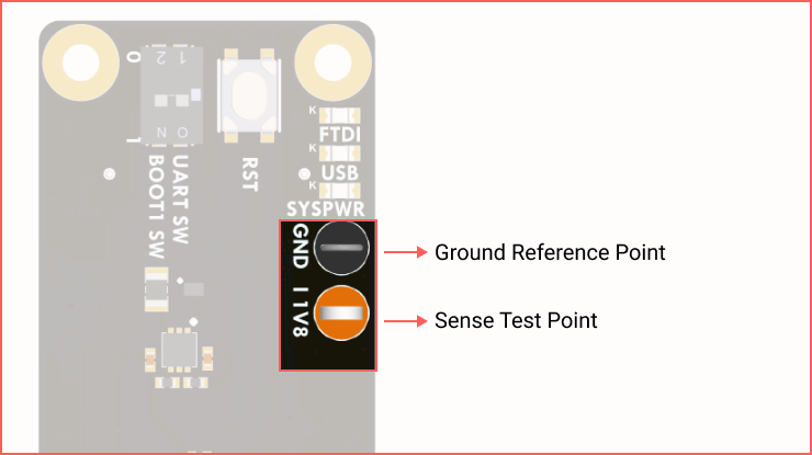
There are two primary test rings designed for power measurement:
Orange Ring: This is the Sense test point. It outputs a voltage proportional to the current being drawn by Pulsar.
Grey/Black Ring: This is the Ground (GND) reference point for the measurement.
How It Works
Pulsar operates on a single 1.8V power rail. A 3 Ohm high-side shunt resistor is included to enable current measurement on this rail. A factor of 25 V/V amplifies the voltage drop across this resistor and can be measured at the orange Sense test point.
How to Take a Reading
Users can measure Pulsar’s power consumption using a standard multimeter or an oscilloscope for more dynamic readings.
Connect the positive probe of the multimeter/oscilloscope to the orange (Sense) test ring.
Connect the negative (ground) probe to the grey/black (Ground) test ring.
The device will display a voltage reading, typically in the range of 50 mV to 1000 mV (1V), depending on the chip’s activity.
Calculating Pulsar’s Current Draw
To find the actual current (in Amperes) being consumed by Pulsar, the user needs to divide the measured sense voltage by 75.
Current Draw Formula:
(This factor comes from the shunt resistor’s value multiplied by the amplification factor -> 3 Ω * 25 V/V = 75)
Example:
Measured Voltage: 750 mV (or 0.750 V)
Calculation: 0.750 V / 75 = 0.01 A