Pulsar Spiking Neural Processor Datasheet
1. Introduction
Pulsar, also known as C1, is a versatile and programmable neuromorphic System-on-Chip (SoC) designed as a flexible platform for ultra-low-power inference acceleration at the edge. It is designed to be sensor-agnostic, enabling the creation of comprehensive, end-to-end solutions across various applications and sensor modalities, including audio, radar, IMU, EMG, ECG, and DVS or low-resolution camera inputs. Pulsar efficiently transforms raw sensor data into actionable insights by integrating a sophisticated, ultra-low-power Spiking Neural Network (SNN) engine, featuring a combination of 12 digital and 4 Analog SNN cores, with a 32-MAC Tiny Convolutional Neural Network (CNN) accelerator for conventional AI tasks. This heterogeneous architecture is further augmented by a 32-bit RISC-V processor core with floating-point support, enabling Pulsar to manage custom workloads, orchestrate complex data flows, perform system housekeeping, and coordinate real-time actions.
Download Pulsar Datasheet Here
Figure 1: Pulsar Spiking Neural Processor
Key architectural features in Pulsar include a 1024-point FFT/iFFT accelerator, dual advanced Scatter-Gather DMA controllers, and hardware barriers, all contributing to a single-chip solution optimised for efficient signal pre-processing, feature extraction, sensor fusion, AI-driven inference, and responsive real-time operation. To ensure seamless integration and minimise Bill of Materials (BOM), Pulsar incorporates on-chip LDOs, an on-chip PLL, support for an external oscillator, and a comprehensive suite of standard interfaces compatible with a wide array of commonly used sensors and peripherals.
Unique Value Propositions
Heterogeneous AI Acceleration at the Edge: Combines ultra-low-power SNN cores with a CNN accelerator and an FFT/iFFT engine for comprehensive on-chip processing from sensor to insight.
Optimised Power Efficiency: Pulsar features multiple power domains, advanced clock gating, several sleep modes, on-chip LDOs, and low voltage operation (down to 0.65V) for minimal energy consumption in always-on and battery-powered applications.
Enhanced Data Flow Management: This technology incorporates dual advanced Scatter-Gather DMAs and hardware barriers to automate and accelerate complex data movement and synchronisation between processing elements, memory, and peripherals.
Flexible and Stand-Alone SoC: This integrated system incorporates a RISC-V CPU, ample embedded SRAM (384 KB main, 32 KB AON retention), OTP memory, and a rich set of digital and Analog I/O interfaces, enabling standalone operation and reducing external component requirements.
Comprehensive Connectivity and Sensor Agnosticism: It offers a wide array of peripheral interfaces, including QSPI (Master/Slave), I2C, I2S, UART, PDM2PCM, parallel camera interface, and ADCs, ensuring compatibility with a diverse range of sensor types.
Simplified Development and Deployment: Supported by a Pytorch-based machine learning framework, network compilers, and a GCC-based SDK for straightforward development, debugging, and deployment of complex AI models directly from Python to hardware.
Minimised Bill of Materials (BOM): Achieved through on-chip LDOs, an on-chip PLL, and support for an external oscillator, reducing the need for external power management components.
2. Key Features
2.1. Compute Engines
Spiking Neural Network (SNN) Accelerators:
Pulsar integrates a powerful hybrid SNN engine, combining 12 digital SNN cores with 4 Analog SNN cores. This engine is designed for highly efficient, event-driven processing of spatiotemporal data. This dual approach allows for a flexible balance between the ultra-low power capabilities of Analog SNNs and the scalability of digital SNNs.
Each of these 16 SNN cores supports up to 4K synaptic parameters, enabling the implementation of complex neural network topologies.
The SNN architecture is optimised for ultra-low-power consumption, making it ideal for always-on sensing applications and battery-operated devices.
The digital SNN (DNR) cores operate on a dedicated auxiliary clock, independent of the main system clock, to enhance energy efficiency.
Hardware Data-to-Spike Encoders facilitate direct digital-value interface to the SNN fabric. The user can select any combination between three types of encoders: integrate & fire, temporal contrast and rate.
Convolutional Neural Network (CNN) Accelerator:
A dedicated “Tiny CNN” accelerator with 32 Multiply-Accumulate (MAC) units per cycle provides hardware acceleration for conventional deep learning operations, typically used for feature extraction in Pulsar.
The CNN accelerator operates with 8-bit precision, striking a balance between computational efficiency and model accuracy for edge AI tasks.
RISC-V CPU Core:
At the heart of Pulsar is a 32-bit RISC-V processor core, equipped with a Floating Point Unit (FPU) for handling complex calculations.
The CPU’s instruction set is extended and optimised for improved hardware utilisation and control within the SoC. It manages system configuration, orchestrates data flow, handles housekeeping tasks, and can execute custom application kernels.
FFT/iFFT Accelerator:
Dedicated hardware accelerator for FFT/iFFT calculations (up to 1024-point).
Operates at a maximum frequency of 160 MHz.
Designed for efficient on-chip pre-processing of sensor data (e.g. audio, radar).
Features dedicated DMA for high-throughput data handling.
Supports configurable data-type conversion (floating-point to fixed-point).
2.2. Memory System
Embedded SRAM:
Pulsar incorporates 384 KB of on-chip embedded SRAM for general-purpose use, including code execution, data storage, and intermediate results from processing engines.
This main memory is organised with interleaved banks, which significantly enhances throughput by allowing concurrent accesses from multiple system masters.
Always-On (AON) Retention SRAM:
A dedicated 32 KB block of Always-On (AON) Retention SRAM is available. This memory is designed to retain critical data even during Pulsar lowest power sleep modes, enabling faster wake-up times and preserving system state.
CNN Scratchpad & Instruction SRAM:
The CNN accelerator is supported by 128 KB of dedicated scratchpad SRAM for storing feature maps and intermediate data, minimising data movement and power consumption.
Additionally, 4 KB of dedicated instruction SRAM is provided for the CNN accelerator.
FFT SRAM:
The FFT/iFFT accelerator has access to 93 KB of dedicated SRAM for its operations.
Boot ROM:
A 16 KB Boot ROM securely stores the initial bootloader code and system initialisation routines.
One-Time Programmable (OTP) Memory:
32 Kb of OTP memory is integrated, allowing for permanent storage of essential device-specific data such as calibration parameters, unique identifiers, or security keys.
Advanced Scatter-Gather Direct Memory Access (SG-DMA):
Pulsar features two advanced Scatter-Gather DMA (SG-DMA) controllers. These significantly improve data transfer efficiency, especially for non-contiguous data blocks common in AI and sensor processing, by automatically allowing data to be gathered from or scattered to multiple memory locations. This reduces CPU overhead and improves overall system performance.
Hardware Barriers:
Hardware barriers, including Event Bridge Barriers, are implemented to facilitate synchronised and automated data-flow management between the various processing engines, memory, and peripherals. This ensures data coherency and efficient pipeline processing without continuous CPU intervention.
2.3. Real-Time Features & Control
Interrupt & Event Management:
Arbitrates between 64 hardware maskable interrupts.
The system supports 15 software-triggered events, providing a flexible mechanism for inter-process communication and signalling within applications.
Event-based context switching, which can operate independently of the CPU, enables rapid responses to critical system events and efficient management of processing states.
Hardware Semaphores:
Integrated hardware semaphores provide a reliable mechanism for resource locking and synchronisation between the RISC-V CPU, the AI accelerators, and other peripherals, preventing race conditions and ensuring data integrity in a multi-master system.
Timers:
Advanced Timers (2x): Two 32-bit advanced timers are available for generating PWM signals and other precise timing events.
General Purpose Timers (2x): Two 32-bit general-purpose timers are provided, which can be combined to function as a single 64-bit timer for extended time-keeping requirements.
Watchdog Timer (WDT): A 32-bit watchdog timer is included to ensure system reliability by triggering a reset in case of a software malfunction.
System Tick Timer (SysTick): A 24-bit system tick timer is provided for operating system (OS) task scheduling and other system time-keeping functions.
I/O Event Mapping & Triggering:
GPIO pins can be mapped to external interrupt vectors, enabling the system to respond quickly to changes in external signals.
Pulsar also supports event triggering directly through its GPIO pins, enabling GPIO state changes to initiate specific actions or signal events within the SoC.
2.4. Peripheral Interfaces & Connectivity
Memory & Storage Interfaces:
Two Master Quad SPI (QSPI) controllers facilitate high-speed serial communication, primarily interfacing with external flash memories for code storage and data logging.
One Slave Quad SPI (QSPI-S) controller allows Pulsar to act as a QSPI peripheral device, enabling it to be controlled or accessed by an external host processor or system.
Communication Interfaces:
One Inter-Integrated Circuit (I2C) master interface provides a standard 2-wire serial bus for connecting to a wide range of sensors, EEPROMs, and other low to medium-speed peripherals.
A single Universal Asynchronous Receiver-Transmitter (UART) interface provides a flexible serial communication port for debugging, console access, or interfacing with other devices that support the UART protocol.
Audio Interfaces:
An Inter-IC Sound (I2S) interface is available for direct connection to digital audio codecs, microphones, or other audio integrated circuits (ICs), supporting standard digital audio streaming protocols.
A Pulse Density Modulation to Pulse Code Modulation (PDM2PCM) audio interface allows for direct connection of PDM digital microphones. It internally converts their output to the standard PCM format, simplifying audio front-end design.
Camera Interface:
An 8-bit parallel camera interface (CIF) is provided for connecting to image sensors or event-based cameras. It supports a configurable data bus (4-bit or 8-bit), hardware synchronisation signals (hsync/vsync), and on-the-fly image scaling through decimation, facilitating efficient visual data acquisition. (New in Pulsar)
General Purpose I/O (GPIO):
Pulsar offers 20 programmable GPIO pads, providing flexible digital input and output capabilities.
Each GPIO pin supports individual software configuration for up to 4 alternate peripheral functions via a flexible I/O muxing scheme, allowing optimal pin utilisation based on application requirements.
These GPIOs can also be configured as external interrupt sources.
Analog Front-End:
Two dual-channel front-end Analog-to-Digital Converters (ADCs) are integrated, enabling direct digitisation of Analog signals from various sensors without requiring external ADC components.
PWM Encoders/Decoders:
Four Pulse Width Modulation (PWM) units are available. These can be configured as encoders to generate PWM signals for motor control or other applications or decoders to interpret incoming PWM signals.
Debugging Interface:
A standard Joint Test Action Group (JTAG) interface provides comprehensive on-chip debug and test capabilities, essential for software development and hardware verification.
2.5. Power Management
Optimised Design for Low Power:
Pulsar incorporates an internal low-power Phase-Locked Loop (PLL) for generating system clocks efficiently.
Power consumption is minimised through the extensive use of fine-grained, individual clock gating for each functional block, ensuring that inactive modules do not draw unnecessary power.
The architecture features multiple, distinct power domains that can be managed independently. This allows unused chip sections to be powered down, saving energy.
On-chip Low-Dropout (LDO) regulators generate the necessary internal core and Analog voltage supplies from the main 1.8V input. These LDOs are software-controllable, offering flexibility in power management strategies.
The design supports low-voltage operation for core logic, down to 0.65V, further enhancing overall power efficiency, which is critical for battery-powered devices.
Flexible Sleep Modes:
Pulsar offers three software-controllable sleep modes to cater to various low-power application scenarios. These modes provide a tiered approach to power saving:
Soft Sleep: The main system clock is gated off, significantly reducing dynamic power while allowing quick resumption of activity.
Light Sleep: Extends power savings by managing power to specific blocks while preserving critical data, such as that in the 32KB AON Retention SRAM.
Deep Sleep: Maximises power savings by turning off most on-chip power domains, suitable for extended periods of inactivity.
2.6. Boot Modes
Flexible Boot Options: Pulsar provides a range of boot modes, offering versatility in system startup and firmware loading from various sources:
JTAG: Allows booting and debugging via the JTAG interface, typically used during development and testing.
UART: The UART interface enables booting from an external host, and it is often used for initial programming or recovery.
Master SPI (Single SPI): This mode enables the system to boot directly from a standard external SPI flash memory. The “Single” designation distinguishes it from Dual or Quad SPI protocols and utilises the conventional 4-wire interface (SCLK, CS, MOSI, MISO). This mode automatically tweaks its communication speed during boot-up, so you get a faster start-up.
Master QSPI (Quad SPI): This mode supports booting from an external QSPI flash memory using four data wires for higher throughput. The communication speed for this mode is automatically adjusted during the boot-up sequence for faster boot time.
Slave SPI (single SPI): This mode allows Pulsar to be booted by an external host processor acting as an SPI master.
2.7. Software Development Ecosystem
Comprehensive Toolchain for AI Development: Pulsar is supported by an extensive suite of software tools designed to simplify the development and deployment of AI applications:
PyTorch-Integrated Machine Learning Framework (Talamo SDK): This framework, deeply integrated with PyTorch, provides a high-level, user-friendly environment for designing, training, and optimising both Spiking Neural Networks (SNNs) and Convolutional Neural Networks (CNNs) targeted for Pulsar.
Dedicated Network Compilers & Mappers: Specialised compilers and mappers are provided for SNNs and CNNs. These tools translate the trained neural network models from the Python-based development environment into an optimised hardware configuration for efficient execution on Pulsar’s dedicated accelerators.
TensorBoard Integration for Performance Visualisation: Developers can leverage TensorBoard to visualise key network performance metrics, such as accuracy, latency, and resource utilisation, which aids in debugging, fine-tuning models, and understanding hardware interactions.
Talamo SDK: A comprehensive Software Development Kit (SDK) underpins application development on Pulsar. It includes hardware abstraction layers (HAL), drivers for on-chip peripherals, libraries for standard functions, and examples to accelerate the development process.
Embedded SDK for Low-Level Programming (SPINE): An embedded SDK provides developers with resources that require fine-grained control over hardware resources and low-level programming capabilities.
Standard RISC-V GCC Toolchain: The RISC-V CPU core is equipped with a comprehensive GNU Compiler Collection (GCC)-based toolchain, enabling development in C, as well as access to standard libraries and debugging tools for the CPU’s general-purpose processing tasks.
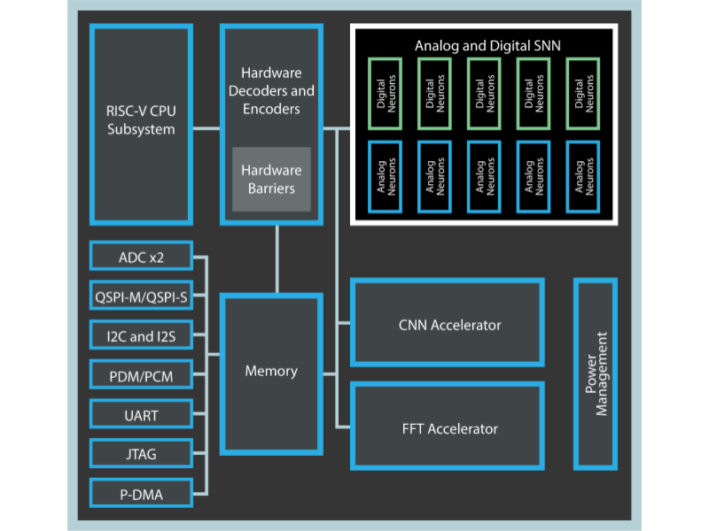
3. Architecture Overview
This section provides a high-level overview of Pulsar Spiking Neural Processor’s architecture, illustrating the primary functional subsystems and their interconnectivity. Pulsar utilises a combination of different processor types, including a RISC-V CPU and specialised engines, to efficiently manage various tasks such as gathering data from sensors, processing that data, executing AI processes, and controlling the system.
3.1. High-Level Block Diagram
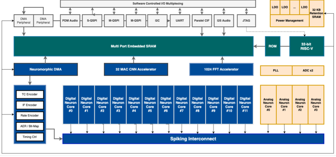
Figure 2: A labelled block diagram of Pulsar product architecture.
The Pulsar System-on-Chip (SoC) architecture is designed for versatile and power-efficient edge AI processing. At its heart is a 32-bit RISC-V processor that works in conjunction with a central Multi-Port Embedded SRAM. The architecture integrates several specialized hardware accelerators, including a 32 MAC CNN Accelerator and a 1024-point FFT Accelerator, which interface directly with the central SRAM.
For neuromorphic workloads, Pulsar features a hybrid engine of 12 Digital Neuron Cores and 4 Analog Neuron Cores. These are linked via a dedicated Spiking Interconnect and are fed by a data path that includes a Neuromorphic DMA and specialized hardware encoders (TC, IF, Rate).
A rich set of peripheral interfaces, such as QSPI, I2C, UART, and I2S Audio, provide versatile connectivity, managed through Software Controlled I/O Multiplexing. The system is completed by essential components including a Power Management block with LDOs, on-chip ROM, a PLL for clock generation, and dual ADCs for analog sensor interfacing
This document has been truncated for RST conversion. Please continue with remaining sections for complete coverage.